Blog

Contact

Pin-Out Challenge: Re-think the Solution

Interview with Cherie Litson by Tara Dunn

Semi-Additive PCB fabrication is getting a lot of attention, as fabricators install new processes enabling them to provide much finer features than traditional subtractive etch processes. This is opening new opportunities and tools for PCB designers to solve today’s complex electronics challenges. These package and interconnect solutions can reduce size and weight by 90% over traditional processing techniques in the U.S. and bring signficant signal integrity benefits. As with any new technology, there are many questions: how to apply this new capability to the design, what are the signal integrity considerations, who has the capability to supply these fine features?

This column is kicking off a series of interviews with veteran PCB designers: getting their thoughts, opinions and questions as they navigate this new frontier. Today, I am sitting down with Cherie Litson, MIT CID/CID+ President of Litson1 Consulting, and an Instructor at Everett Community College, to understand her perspective on this new fabrication capability.

Tara Dunn: Cherie, you are a well-known designer and instructor in the industry, but for those who have not had the opportunity to meet you, could you please start with a quick introduction?

Cherie Litson: My background is broad and deep: it has been an amazing opportunity to work with so many companies, notably Microsoft – where I helped create their design database for the Surface and earlier, the first wireless mouse. The first hand-held ultrasound from SonoSite was another passion project. Passing on what I have learned from others lead me to becoming a Master Instructor for the IPC Designer Certification program. I learn more every time I teach! As a member of the Averatek Community of Interest, I encourage everyone in the industry to share their experiences with this new technology – so we can all learn and optimize the benefits of new developments.


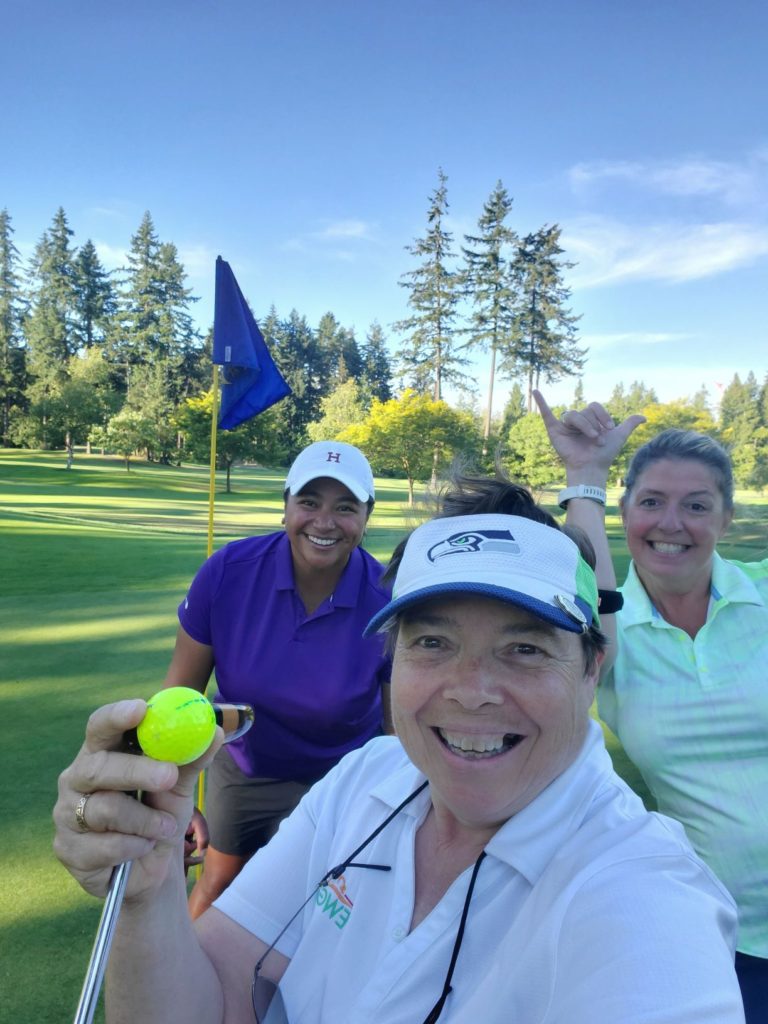
Golf is my other passion: I have been involved in the LPGA Amateur
Association (previously EWGA) since 2001. While learning how golf and the professional
world mix, I have been able to take my golfing teams from local to national
competitions for the past five years. I could go on about golf, but let’s tee
up this discussion!


Dunn: Impressive! My golf skills stop with my highly
developed golf cart driving expertise; actually hitting that ball in a straight
line is something I am still working on. You mention Averatek’s Community of
Interest; this is new. Can you tell me about that?

Litson: Averatek, a Silicon Valley innovation company,
manufactures key chemistries and licenses the processes for their use. Two
processes, in particular, are having an effect on the PCB design industry:
LMITM, the catalytic ink used in the A-SAP™ process, and Mina™, a surface
treatment that enables soldering to aluminum. These products are now
commercially available through licensed fabricators, so it is important for
designers to learn about them. The Community of Interest is starting to
bring together a wide range of people from all sectors of the industry who are
interested in learning more about semi-additive PCB processes. Nothing formal
yet, but we’re hoping to set up a website or blog to pool our knowledge on
these types of products.

Dunn: What aspect of these new PCB fabrication capabilities
is most valuable to you?

Litson: I am excited by the ability to route traces at 1
mil or even below, as that opens possibilities for designers to produce
increased density at lower cost. The A-SAP process provides the designer an
opportunity to significantly reduce layer count, simplifying complex designs.
These geometries can potentially eliminate pin-out challenges while maintaining
reliable signal integrity. I can see the advantages of using a taller yet
narrower trace for signal integrity; this is the winning factor for me. This
process results in traces with vertical rather than trapezoidal sidewalls,
realizing benefits in both size and RF advantages, eliminating the etch
compensation requirements. Designers working on next-generation products will
be excited about the ability to form a 15-µm trace and space with the
semi-additive processes. Many designs are being driven to require line and
spaces at 50 µm due to smaller pin spacing on components and smaller package
products. The fabrication of these traces is something that has not been
available in the U.S. until now.

Dunn: Cherie, I know you are an avid learner; when you are
researching new technology, which reliability tests mean the most to you?

Litson: As I consider how to best apply this technology,
material compatibility is an important aspect. It is important to know that a
new process is going to be compatible with nearly all materials. Next, I’m
looking into the electrical aspects of these new geometries. I also look at
proven reliability parameters: the A-SAP process passed peel strength, IST
coupon testing, and signal integrity analysis across a variety of
materials. 

Dunn: Working with something new can be exciting and just a
little intimidating. Navigating the learning curve, do you see any challenges
for designing with this new technology in mind?

Litson: In my opinion, designers should remember their
basic electronics—it influences everything we do. We must understand the
physics to make certain we know what will be affected. With these new
parameters, we will need to go back and take another look at our calculations,
which are based on the resistance of copper which is based on the area. Then
bring into the equations the resistance of the dielectric materials, layer
structures, etc. I am curious to see how the geometry of the conductors shifts
the electrical results. Because each product is different, there are few
set-in-stone design rules for semi-additive processed layer-only guidelines.
The most important guideline: this process requires close collaboration between
design and fabrication. For additional guidance, a collection of case studies
would be great, maybe online as a dynamic design guide. Just brainstorming!

Dunn: An online dynamic design guide is a great idea.
Taking a step back from design, why do you feel that this new technology is
important to the industry?

Litson: I think this is important to the industry for
several reasons. One is implementation of this process—it is designed to
integrate with existing PCB fabrication equipment, so it does not require the
costly capital investment usually associated with new technologies, allowing
even the smaller and mid-size shops to offer this advanced technology to their
customers. While this process certainly gives us the benefit of 25 µm
line/space and below, the additive process also has RF benefits at larger
feature sizes, such as improving impedance control. I think we are just
scratching the surface of how to get the most benefit from this capability. I
am already seeing the simplification of complex designs, improving yields, and
reducing costs. I am excited to see where this technology takes us.

Dunn: Cherie, as we wrap up, what advice would you give to
PCB designers who are just hearing about the opportunity to work with
fabricators that can now offer these fine feature sizes?

Litson: Start today! Do some research, share your concerns,
share your experiences, try it out. I can see many benefits to utilizing this
process at the 75 µm, 50 µm, and 25 µm trace sizes and smaller.

Dunn: Thank you so much for talking with me today. To learn
more, what is the best way to reach you?

Litson: The best way to reach me is at Litson1@ aol.com.
Thank you.

Interview with Meredith LaBeau of Calumet Electronics

Calumet Electronics was the very first printed circuit board manufacturing company to commercialize the revolutionary new Averatek Semi-Additive Process (A-SAP™) and offer the ability to manufacture 25-micron feature sizes with PCB technology.  I am sitting down to discuss the A-SAP™ solution with Calumet’s Meredith LaBeau.

Tara Dunn:  Hi Meredith, can you share a few thoughts on your initial reaction to this technology and what factors led to the Calumet Electronics decision to partner with Averatek?

Meredith LaBeau:  Calumet Electronics was first introduced to this technology through an IPC APEX presentation in 2019.  This presentation introduced a new technology that could be utilized to drop the SWaP (size, weight, and power) while still manufacturing printed circuit boards or other advanced packaging in the standard manufacturing and equipment ecosystem. There were many factors that went into the Calumet Electronics decision to partner with Averatek, but at the very top were the following:

  1. The elegance of the solution to advance electronics quickly for domestic advanced technology needs.
  2. The partnership-driven team at Averatek to launch the technology into the domestic marketplace.
  3. The intelligence and support of the Averatek team.
  4. The potential for Calumet Electronics and other PCB manufacturers to have an available solution that is competitive with - and exceeds - the solutions in low-cost regions of the world.

Dunn:  You and your team are doing a fantastic job reaching out and starting discussions with companies that have a need for these fine feature sizes. Throughout these discussions what are a few things that stand out to you, regarding market reaction and receptiveness to a new technology?

LaBeau: In all the discussions, what stands out most is the dire need for a technology that can achieve fine lines and spaces, while also utilizing some of the most advanced HDI features, along with extremely low loss material. These customers often must look overseas for manufacturing, which comes at a cost: long lead times, or re-designing the boards to meet the current domestic technology, often dumbing-down the backbone of the electronics system. 

The Averatek process provides a robust, reliable, and elegant solution to meet the current and next-generation demands sought by the electronic system designers.  These customers, regardless of the end-use market, require advanced PCBs as they continue to advance the electronics requirements along with the IC substrates.  The market is ecstatic about the potential of this technology, providing light at the end of the tunnel for many.

Dunn:  This is an excerpt from you in the A-SAP™ community of interest kick off video.

“The use of this innovative and transformative manufacturing method requires a new approach to design: with manufacturing instead of for manufacturing.  Together, the designer and manufacturer can develop a collaborative approach, to Drop the SWAP - while increasing the reliability and robustness of the PCB for next-generation electronics systems.” 

I often hear you impress on people that collaboration is critical in order to utilize the full potential of the A-SAP™ technology.  How do you facilitate this high-quality communication, and what is your advice for designers who want to get all the advantages of A-SAP™ capabilities?

LaBeau:  When utilizing a transformative manufacturing process, one must fully understand its advantages, as it applies to both design and the product requirements. With a market-changing technology, the manufacturer and designer must work in collaboration to gain all the benefits - while not increasing the cost.

The Averatek process allows a designer to simplify designs by using finer traces and spaces, greater line width control and impedance control. If the designer understands this, you can re-set the technology curve: simplifying designs in order to make the process and end-product more reliable and robust, while reducing risks of lead time or yield delays.

Dunn: Not only has Calumet Electronics invested in Averatek’s A-SAP™ process, but you have also been busy bringing in new materials, new process capabilities, new equipment and even a facility expansion.  It is clear Calumet has a vision for the future.  Do you want to share that vision and some of the exciting new capabilities?

LaBeau: Calumet Electronics does have a driving vision for the future: to advance the technology within the electronics ecosystem, through a combination of standard and new technologies, in partnership with OEMs and electronics assemblers to compete on the world stage.  We want to bring the United States back to designing and manufacturing the most state-of-the-art printed circuit boards to meet the rugged domestic demands.  In concert with this vision, is also our goal to bring engineering back to focus on PCB manufacturing, by working in collaboration to advance Manufacturing Readiness Levels (MRLs) of our customers’ product - from concept to volume production.

Calumet is focused on developing a world class staff to meet the technological needs of the electronics supply chain. In addition, we are focused on the PCBs that must be made domestically, which include applications for RF, microwave, beamforming, high precision tolerancing and fine lines and spaces.

Dunn: One thing that is clear when visiting Calumet Electronics: the pride in and support for the community.  Along that theme, I would like to ask a more personal question. I am fascinated by one of your extra-curricular activities, serving as Director for a 150-mile dogsledding race.  Can you tell us a little about that?   

LaBeau: Living in the Copper Country in Upper Michigan, you come to really understand the concept of community. The harsh winters teach you to dig in, work hard and support your neighbors. This sense of community development endeared me to an organization, the CopperDog 150. This organizational utilizes a sled-dog race to showcase the natural winter beauty around the Copper Country as well as bring folks out together in the community to cheer on the rugged toughness of sled dogs.  I joined the group in 2010 and within a year was assisting the current race director on every facet of a large-scale race and community event. This director happens to now be my boss and mentor, Todd Brassard, our COO.  I eventually took over the reins. For many years I have enjoyed working with these unsung athletes, but most importantly breathing life into the sleepy towns of the Keweenaw Peninsula - to bring in vital tourism and increasing pride of our communities!

Dunn: Meredith, thanks for taking time for this short interview.  For those interested in learning more about Calumet Electronics, what is the best way to reach you?

LaBeau: Thanks for taking time to speak with me today, Tara. Those who are interested in learning more can reach out to me via email at mlabeau@calumetelectronics.com.

Additive Electronics – Next Generation PCB Capabilities

Exciting news! This column marks the launch of a series of columns diving into semi-additive PCB (SAP) manufacturing processes. We will explore topics ranging from SWaP (space, weight, and packaging) benefits, signal integrity benefits, materials characterization, reliability testing, and even the search to find a calculator that is compatible with straight conductor sidewalls and line width and space at 1.0 mil and below.
Although more people are becoming familiar with the term SAP, specifically as it relates to PCB manufacturing, this technology is new to most people. It seems that mSAP (modified semi-additive processes) make headlines for enabling volume consumer applications such as our smartphones, to be produced with roughly 35-micron feature sizes. Yet we have not heard a lot about semi-additive PCB processes for applications outside of this specific market.

The really exciting news is that there are now a handful of U.S.-based fabricators offering this technology for low volume/high mix applications. This opens so many new opportunities previously unavailable for PCB designers and at the same time generates a myriad of questions from the design community as well as the fabrication community. Before we dive in and start addressing these questions, let’s step back and discuss the semi-additive PCB process flow and how that is being integrated into existing subtractive etch PCB processing lines.

Semi-Additive PCB Process
This process flow from Averatek gives a simplistic view of the semi-additive PCB process flow. I do not want to assume that all are familiar with the subtractive etch process and want to point out that with steps two and three, these are the same process steps used to manufacture with traditional processes. Rather than etching away the copper that is not required for the circuitry, with this process, all copper is etched from the manufacturing panel. From there, a palladium deposition using LMI™ technology is coated on the panel. The next step is electroless copper, typically the same electroless chemistry
being used by the fabricator for the subtractive process.

This step is critical to understanding the benefits of the semi-additive process. The thin LMI coating enables a very thin, conformal layer of electroless copper, 4–20 µin, which is much thinner than typical electroless copper plating. More to come on the significance of this.

Following electroless copper, panels move to dry film resist imaging, followed by electrolytic copper and dry film resist strip, all standard manufacturing processes. The final step in the circuit creation process is to flash-etch the electroless copper layer. Circling back to the thickness (or actually, thinness) of that electroless copper layer, it is important to point out that the flash-etch of the very thin electroless copper layer has very little impact on the trace itself. Etching of thicker copper results in the trapezoidal effect that we are all aware of. With semi-additive processing, the trace sidewalls remain straight, and the line
width tolerance is tighter. In future columns we will discuss the impact of this on impedance control.

Following these wet process steps, the semi-additive manufacturing panels will follow the same process flow that subtractive etch panels follow including solder mask, surface finish plating, electrical test, and
inspection.

Why Is This Important to PCB Design?
Traditional subtractive etch processing, at least in the U.S., becomes very difficult for feature sizes below 3 mils (75 microns). As electronics packages shrink, this forces PCB designs to become much more complex— adding extra routing layers, adding microvia layers, and increasing lamination cycles
required, all which impact yield, reliability, and cost.

The semi-additive process jumps this technology curve. Within a few weeks, fabricators previously able to offer 3-mil line/space, can now offer 1-mil line/space and below. That is a complete game changer for PCB design. Some of the benefits are easily seen:


• The ability to shrink the overall size of a circuit
• The ability to route additional traces between pads can reduce the overall number of layers required for a design and subsequently the ability to reduce the number of stacked or staggered microvias

Over the next few months, we will review use cases to help spur ideas.

There are also significant signal integrity benefits from semi-additive processing. There is tighter line width control and straight conductor sidewalls greatly improve impedance control. Another feature to additive processing creating a buzz within the design community is the ability to create higher aspect ratio traces than available with subtractive etch or even mSAP options.

We are just scratching the surface on how to best apply these new capabilities to PCB design, and I am looking forward to collaborative discussion and creativity. It is tempting to ask for “design rules” but in my opinion, that may limit the creativity in approaching design challenges in a new way and my hope is that we can develop a community of interest followed by a community of design expertise around this new technology. Please reach out to me with your questions and stay tuned as we start a deeper dive into this exciting technology.

Very High-Density Interconnect, Be Part of the Community

Averatek’s A-SAP™ Process

2021 is a VERY exciting time for Averatek’s A-SAP™ process.  There are currently three U.S. based fabricators licensing this technology and building panels, opening commercial capacity that has not previously been available in the US.

Ability to Form 15-micron traces and spaces is proven

At this point, the ability to form a 15-micron trace and space with the A-SAP™ process has been well proven.  While gathering reliability data is something that will not ever be “complete”, Averatek is also publishing results of tests including IST coupon testing and signal integrity analysis across a variety of materials.

Now, let’s build a Community of Interest to take advantage of those benefits

The next step that Averatek is excited to announce is the launch of the “A-SAP™ Community of Interest” content platform.  With commercial availability and proven reliability parameters, it is now time to build a community of experts from across all sectors of the electronics industry that understand this technology from a fabrication perspective and understand how to apply this technology to optimize the benefits of 15-micron trace and space in PCB design.  As with any technology advancement, this capability will have impacts across the full supply chain:  materials, design, fabrication, assembly, equipment, and standards.

This exciting semi- additive PCB fabrication process enables high-density PCB design opportunities coupled with RF and signal integrity benefits that were previously unavailable and provides a tremendous benefit to PCB designers.  The installation of A-SAP™ is a relatively simple process that allows fabricators to meet the ever-intensifying HDI needs of their customers.

Video from Industry Experts

The short video, link below, announcing the A-SAP™ Community of Interest platform, lets us hear from several designers and fabricators, in their own words, express why they are excited for this technology breakthrough and why they believe this is important for the industry.

Kelly Dack comments that the design world will need to be prepared to have their small scall design challenges rocked.  Cherie Litson is excited that Averatek’s A-SAP™ process eliminates pin out challenges while maintaining reliable signal integrity and Randy Chase clearly articulates the design requirements that are driving him to require line and spaces at 50 micron, something that is not reliably and repeatedly available in the U.S. today with subtractive etch processes.

Calumet Electronics is the first commercial fabricator to offer this technology.  Dr. Meredith LaBeau expressed her thoughts advocating that designers and manufactures have the opportunity to collaborate to “drop the SWaP” while increasing the reliability and robustness of the most essential component, the printed circuit board.  Brad Bourne, CEO of FTG is excited to work with Averatek’s advanced PCB fabrication process to support their Aerospace and Defense customers for years to come.  Anaya Vardya, CEO of American Standard Circuits sees value in two areas, fine line, sub 2 mil trace and space feature sizes and the ability to form conductors with gold rather than copper conductors, a benefit becoming increasing important to the medical industry.

Materials suppliers play an integral role the PCB fabrication and PCB design process and there are several new materials coming to market.  Material compatibility with A-SAP™ from both peel strength and signal integrity characterization, is something that most everyone is interested in as they consider how to best apply A-SAP™ technology.  Reaching out to Chris Hunrath, Vice President of Technology at Insulectro, he expands on the benefits of using a taller yet narrowing traces for signal integrity advantages, an important factor in this technology breakthrough.  Paul Cooke, Field Applications Engineer and Technical Sales for AGC-Nelco, is now on the materials side of the supply chain, with deep roots in PCB fabrication.  He shares his thoughts on the advantage from both an RF perspective, eliminating the etch comp requirements, and the opportunity to significantly reduce layer count, simplifying complex designs.

Altium’s Director of Community and Industry Engagement, Judy Warner, is excited for the benefits that Averatek’s A-SAP™ process opens up for PCB design engineers including increased density, lower costs and benefits to SWaP.

As Averatek’s Vice President of Marketing and Business Development, I invite you to listen to this short video, visit our website, and join our mailing list to quickly receive new information and updates.  The A-SAP™ Community of Interest Platform will be expanding quickly with content and comments from all areas of the electronics supply chain.  As always if you have any specific questions about this technology, please reach out to me at tara@averatek.com.

Averatek A-SAP™ Community of Interest Content Platform Kick-off video link.

Game Changer: 25-micron trace and space

Can you imagine the benefits of routing a PCB Design with a A-SAP™ 25-micron trace and space?

Just to name a few; complex pin outs could require fewer layers and a reduction in costly lamination cycles, the overall footprint of the PCB could be dramatically reduced, or conversely, additional electronics functionality could be fit into an existing footprint.

This benefits alone is exciting, but NOW just imagine if that 25-micron trace and space technology could be integrated into a PCB stack-up that included both very high-density feature sizes along with traditional subtractive etch technology?   Yes, A-SAP™ processes blend easily with all the traditional circuit fabrication processes.

Imagine This…A-SAP™ layers

To kick start your imagination picture this: a 10-layer printed circuit board design, pushing the traditional design limits of the subtractive etch process, requires stacked or staggered micro vias and three lamination cycles.  We have all been there, right?  Nail-biting hoping for good yields knowing you have designed something that will push boundaries of even your more trustworthy, high technology fabricators.

Here is the good news. This design could be re-imagined using 25-micron trace and space on critical pin out layers, while keeping other layers as originally designed, using the best of both PCB processes and resulting in a reduction in overall size and thickness, specifically, a reduction to 8 layers but perhaps even more importantly, a reduction to just one lamination cycle. Simplifying the fabrication process, increasing yields and reducing costs.  Something to think about!

Averatek’s A-SAP™, a Semi-Additive PCB technology does just that.  A-SAP™ is currently being licensed to printed circuit board fabricators and is now commercially available for prototype and low to medium volume production.  This technology enables the fabrication of 25-micron line and space and below and is relatively easily integrated with traditional PCB fabrication processes, eliminating the need for costly capital investment while allowing these fabricators to leap-frog past traditional PCB capabilities.

This ultra-high-density packaging and interconnect solution can reduce size and weight by 90% over current state of the art processes within the US, is shown to have significant RF advantages over traditional subtractive-etch processing and is opening-up design possibilities that were previously unavailable.

A future blog will go into detail about how the semi-additive PCB process fits within the framework of traditional PCB fabrications processes, but as a sneak peek, rather than creating the circuitry from a traditional copper clad laminate and etching the copper that is not required, this semi-additive process starts by removing all the copper from the base laminate, and then adding copper to the bare substrate creating the specified circuit pattern.

The key lies in the very thin electroless copper layer, significantly thinner than copper foils. Once the circuit image is created, electrolytic copper finishes the circuit plating. Because the initial electroless copper is so thin, much thinner than any of the available foil options, the flash etching to remove the unnecessary copper does not noticeably impact the circuit pattern.

This process results in traces with horizontal sidewalls rather than trapezoidal in shape, realizing benefits in both size and RF properties. Once the circuit pattern is created, the circuit layers follow most of the traditional PCB fabrication steps involved in the subtractive etch process.

Visit our information center at  www.averatek.com to learn more about the A-SAP™ process and the benefits of designing with 25 micron feature sizes.  Please reach out to me at tara@averatek.com if you have any questions.

Information Center

See what’s new.

Ready to learn more?